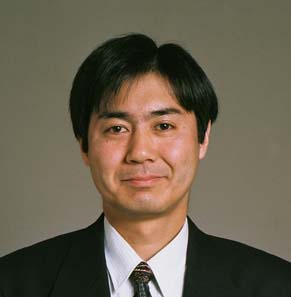
portrait Toshiro Hiramoto received B.S., M.S., and Ph.D degrees in electronic engineering from the University of Tokyo in 1984, 1986, and 1989, respectively. In 1989, he joined Device Development Center, Hitachi Ltd., Ome, Japan, where he was engaged in the device and circuit design of ultra-fast BiCMOS SRAMs. In 1994, he joined Institute of Industrial Science, University of Tokyo, Japan, as an Associate Professor and has been a Professor since 2002. His research interests include low power CMOS devices design, variability in scaled transistors, silicon nanowire transistors, silicon single electron transistors, and silicon power devices.

Dr. Hiramoto is a fellow of Japan Society of Applied Physics and a member of IEEE and IEICE. He served as the General Chair of Silicon Nanoelectronics Workshop in 2003 and the Program Chair in 1997, 1999, and 2001. He was on Committee of IEDM from 1993 to 1994 and from 2003 to 2009. He served as the Program Chair of Symposium on VLSI Technology in 2013 and the General Chair in 2015. He was the Program Chair of International Conference on Solid-State Devices and Materials (SSDM) in 2016.


Present Position:
Professor
Institute of Industrial Science
University of Tokyo

Present Address:
Institute of Industrial Science, University of Tokyo,
4-6-1 Komaba, Meguro-ku, Tokyo 153-8505, Japan

Education:
Ph.D., Electronic Engineering, University of Tokyo, 1989.
M.S., Electronic Engineering, University of Tokyo, 1986.
B.S., Electronic Engineering, University of Tokyo, 1984.

Academic Experiences:
Professor, University of Tokyo, 2002-present.
Associate Professor, University of Tokyo, 1994-2002
Visiting Researcher, Stanford University, 1993-1994.

Industrial Experiences:
Engineer, Device Development Center, Hitachi Ltd., Japan, 1989-1994

Professional Society Activities:
International Electron Devices Meeting (IEDM)
Subcommittee on Integrated Circuits, 1993-1994.
Subcommittee on CMOS Devices, 2003 - 2004.
Subcommittee Chair on CMOS Devices, 2005.
Asian Arrangement Co-Chair, 2006, 2007.
Publications Chair, 2008
Emerging Technologies Chair, 2009
IEEE International SOI Conference
Program Committee, 2000 - 2002.
Short Course Chair, 2003.
Treasurer and Registration Chair, 2004.
Local Arrangements Chair, 2005.
Technical Program Chair, 2006.
General Chair, 2007.
Publicity & Development Chair, 2008
Advisory Committee, 2009 - 2011
Silicon Nanoelectronics Workshop
Program Committee, 1996, 1998, 2000, 2002, 2004 - 2011.
Program Chair, 1997, 1999, and 2001.
General Chair, 2003.
Symposium on VLSI Technology
Program Committee, 2001 - present.
International Symposium on Solid-State Devices and Materials (SSDM)
Steering Committee Vice Chair, 2005.
Steering Committee Chair, 2006.
IEEE Electron Device Society
Elected AdCom Member, 2001 - 2006.
Membership Committee, 1996 - present.
Nanotechnology Technical Committee, 2001 - 2006.
Nanotechnology Council, Nanofabrication Committee, 2002 - present.
Japan Society of Applied Physics (JSAP)
Program Subcommittee Chair on Applied Physics, 2000 - 2002.
Silicon Technology Division, Chair on ULSI Devices, 2003 - present.
Japan Electronics & Information Industry Assoc. (JEITA)
Chair on Ultimate CMOS Committee, 2003 - 2005.
Chair on Nanoscale Device Committee, 2005 - present.
Semiconductor Technology Roadmap Committee in Japan, WG6: PIDS, 2000 - 2010.
Semiconductor Technology Roadmap Committee in Japan, WG12: ERD, Leader, 2006 - present.

Fields of Research Interests:

(1) Low power and low voltage CMOS devices and circuits
- Device/circuit cooperative scheme for ultra-low power VLSI2000 CICC
- DTMOS with high body effect factor1998 IEDM, 2001 TED
- Quasi-planar triangular wire channel MOSFETs2001 SOI Conf
- Multi-gate MOSFETs with sufficient body effect2006 TED
- Variable body factor SOI MOSFETs for low power VLSI2006 IEDM
(2) Physics in scaled MOSFETs
- Quantum mechanical narrow channel effects in nano-MOSFETs1999 IEDM, 2000 EDL
- New device design using quantum effect in narrow MOSFETs2001 IEDM
- Impurity number and position fluctuations in scaled MOSFETs2000 TED
- Mobility enhancement in ultra-thin body pMOSFETs2005 VLSI
- Mobility enhancement by volume inversion in thin body nMOSFET2005 IEDM
- Direction dependence of nanowire MOSFETs2006 IEDM
(3) Silicon nanotechnology and single-electron devices
- Integration of SETs by controlling the oscillation peak1999 IEDM
- Quantum effects in silicon SETs1998 IEDM, 1997 APL
- Silicon dot memory using ultra-narrow channel2002 IEDM, 2003 APL
- Largest oscillations and highly functional Operation of SETs at RT2003 IEDM
- Integration of two-bit-per-cell silicon nanocrystal memory cells2003 IEDM, 2004 EDL
- Double-gate silicon nanocrystal memory2004 SNW
- Analog pattern matching applications of SETs at RT2004 IEDM
- Direction dependence of SETs and largest oscillations 2006 IEDM

CICC: Custom Integrated Circuits Conference
SSDM: International Conference on Solid State Devices and Materials
IEDM: International Electron Devices Meeting
TED: IEEE Transactions on Electron Devices
EDL: IEEE Electron Devices Letters
SNW: Silicon Nanoelectronics Workshop
APL: Applied Physics Letters
VLSI: Symposium on VLSI Technology

Main publications

I. IEDM

  1. T. Hiramoto, N. Tamba, M. Yoshida, T. Hashimoto, T. Fujiwara, K. Watanabe, M. Odaka, M. Usami, and T. Ikeda, "A 27 GHz Double Polysilicon Bipolar Technology on Bonded SOI with Embedded 58 µm2 CMOS Memory Cells for ECL-CMOS SRAM Applications", IEDM, pp. 39 - 42, December, 1992.
  2. H. Ishikuro and T. Hiramoto, "Influence of Quantum Confinement Effects on Single Electron and Single Hole Transistors", IEDM, pp. 119 - 122, December, 1998.
  3. M. Takamiya and T. Hiramoto, "High Performance Electrically Induced Body Dynamic Threshold SOI MOSFET (EIB-DTMOS) with Large Body Effect and Low Threshold Voltage", IEDM, pp. 423 - 426, December, 1998.
  4. H. Majima, H. Ishikuro, and T. Hiramoto, "Threshold Voltage Increase by Quantum Mechanical Narrow Channel Effect in Ultra-Narrow MOSFETs", IEDM, pp. 379 - 382, December, 1999.
  5. N. Takahashi, H. Ishikuro, and T. Hiramoto, "A Directional Current Switch Using Silicon Single Electron Transistors Controlled by Charge Injection into Silicon Nano-Crystal Floating Dots", IEDM, December, 1999.
  6. H. Majima, Y. Saito, and T. Hiramoto, "Impact of Quantum Mechanical Effects on Design of Nano-Scale Narrow Channel n- and p-type MOSFETs", IEDM, pp. 733 - 736, 2001.
  7. M. Saitoh, H. Majima, and T. Hiramoto, "Effects of ultra-narrow channel on characteristics of MOSFET memory with silicon nanocrystal floating gates", International Electron Devices Meeting (IEDM), San Francisco, CA, USA, pp. 181 - 184, December, 2002.
  8. Masumi Saitoh and Toshiro Hiramoto, "Room-Temperature Operation of Highly Functional Single-Electron Transistor Logic Based on Quantum Mechanical Effect in Ultra-Small Silicon Dot", 2003 International Electron Devices Meeting (IEDM), Washington DC, USA, December, 2003.
  9. Il-Gweon Kim, Kosuke Yanagidaira, and Toshiro Hiramoto, "Integration of Fluorinated Nano-Crystal Memory Cells with 4.6F2 Size by Landing Plug Polysilicon Contact and Direct-Tungsten Bitline", 2003 International Electron Devices Meeting (IEDM), Washington DC, USA, December, 2003.
  10. Masumi Saitoh, Hidehiro Harata, and Toshiro Hiramoto, "Room-Temperature Demonstration of Integrated Silicon Single-Electron Transistor Circuits for Current Switching and Analog Pattern Matching", IEEE Electron Devices Meeting (IEDM), San Francisco, USA, pp. 187 - 190, December, 2004.
  11. Gen Tsutsui, Masumi Saitoh, Takuya Saraya, Toshiharu Nagumo, and Toshiro Hiramoto, "Mobility Enhancement due to Volume Inversion in (110)-oriented Ultra-thin Body Double-gate nMOSFETs with Body Thickness less than 5 nm", International Electron Devices Meeting (IEDM), Washington D.C., USA, pp. 747 - 750, December, 2005.
  12. Tetsu Ohtou, Takuya Saraya, Kimiaki Shimokawa, Yasuhiro Doumae, Yoshiki Nagatomo, Jiro Ida and Toshiro Hiramoto, gExperimental Demonstrations of Superior Characteristics of Variable Body-Factor (ƒÁ) Fully-Depleted SOI MOSFETs with Extremely Thin BOX of 10nmh, IEEE International Electron Devices Meeting (IEDM), San Francisco, CA, USA, pp. pp. 877 - 880 December, 2006.
  13. Masaharu Kobayashi and Toshiro Hiramoto, gExperimental Study on Quantum Structure of Silicon Nano Wire and Its Impact on Nano Wire MOSFET and Single-Electron Transistorh, IEEE International Electron Devices Meeting (IEDM), San Francisco, CA, USA, pp. 1007 - 1009, December, 2006.
  14. K. Takeuchi, T. Fukai, T. Tsunomura, A. T. Putra, A. Nishida, S. Kamohara, and T. Hiramoto, "Understanding Random Threshold Voltage Fluctuation by Comparing Multiple Fabs and Technologies", International Electron Devices Meeting (IEDM), Washington Hilton, Washington D. C., USA, pp. 467 - 470, December 11, 2007.
  15. Ken Shimizu, Takuya Saraya and Toshiro Hiramoto, "Experimental Investigation on the Origin of Direction Dependence of Si (110) Hole Mobility Utilizing Ultra-Thin Body pMOSFETs", IEEE International Electron Devices Meeting (IEDM), San Francisco, CA, USA, pp. 67 - 70, December 15, 2008.
  16. Jiezhi Chen, Takuya Saraya, and Toshiro Hiramoto, "Electron Mobility in Multiple Silicon Nanowires GAA nMOSFETs on (110) and (100) SOI at Room and Low Temperature", IEEE International Electron Devices Meeting (IEDM), San Francisco, CA, USA, pp. 757 - 760, December 17, 2008.
  17. Jiezhi Chen, Takuya Saraya, and Toshiro Hiramoto, "Electron Mobility in Multiple Silicon Nanowires GAA nMOSFETs on (110) and (100) SOI at Room and Low Temperature", IEEE International Electron Devices Meeting (IEDM), San Francisco, CA, USA, pp. 757 - 760, December 17, 2008.
  18. YeonJoo Jeong, Jiezhi Chen, Takuya Saraya, and Toshiro Hiramoto, "Uniaxial Strain Effects on Silicon Nanowire pMOSFET and Single-Hole Transistor at Room Temperature", IEEE International Electron Devices Meeting (IEDM), San Francisco, CA, USA, pp. 761 - 764, December 17, 2008.
  19. Ken Shimizu, Takuya Saraya, and Toshiro Hiramoto, "Physical Understandings of Si (110) Hole Mobility in Ultra-Thin Body pFETs by <110> and <111> Uniaxial Compressive Strain", International Electron Devices Meeting (IEDM), Baltimore, MD, USA, pp. 473 - 476, December 8, 2009.
  20. X. Song, M. Suzuki, T. Saraya, A. Nishida, T. Tsunomura, S. Kamohara, K. Takeuchi, S. Inaba, T. Mogami, and T. Hiramoto, "Impact of DIBL Variability on SRAM Static Noise Margin Analyzed by DMA SRAM TEG", International Electron Devices Meeting (IEDM), San Francisco, CA, USA, pp. 62 - 65, December 6, 2010.
II. IEEE Journals
  1. H. Majima, H. Ishikuro, and T. Hiramoto, "Experimental Evidence for Quantum Mechanical Narrow Channel Effect in Ultra-Narrow MOSFETs", IEEE Electron Device Letters, Vol. 21, No. 8, pp. 396 - 398, August, 2000.
  2. Y. Yasuda, M. Takamiya, and T. Hiramoto, "Separation of Effects of Statistical Impurity Number Fluctuations and Position Distribution on Vth Fluctuations in Scaled MOSFETs", IEEE Transactions on Electron Devices, Vol. 47, No. 10, pp. 1838 - 1842, October, 2000.
  3. M. Takamiya and T. Hiramoto, "High Drive-Current Electrically Induced Body Dynamic Threshold SOI MOSFET (EIB-DTMOS) with Large Body Effect and Low Threshold Voltage", IEEE Transactions on Electron Devices, Vol. 48, No. 8, pp. 1633 - 1640, August, 2001.
  4. Masumi Saitoh, Tasuku Murakami, and Toshiro Hiramoto, "Effects of Oxidation Process on the Tunneling Barrier Structures in Room-Temperature Operating Silicon Single-Electron Transistors", IEEE Transactions on Nanotechnology, Vol. 1, No. 4, pp. 214 - 218, December, 2002.
  5. H. Im, T. Inukai, H. Gomyo, T. Hiramoto, and T. Sakurai, "VTCMOS characteristics and its optimum conditions predicted by a compact analytical model", IEEE Transactions on Very Large Scale Integration (VLSI) Systems, pp. 755 - 761, October, 2003.
  6. Masumi Saitoh, Tasuku Murakami, and Toshiro Hiramoto, "Large Coulomb Blockade Oscillations at Room Temperature in Ultra-Narrow Wire Channel MOSFETs Formed by Slight Oxidation Process", IEEE Transactions on Nanotechnology, Vol. 2, No. 4, 4, December, 2003.
  7. G. Tsutsui, T. Nagumo, and T. Hiramoto, "Enhancement of Adjustable Threshold Voltage Range by Substrate Bias Due to Quantum Confinement in Ultra Thin Body SOI pMOSFETs", IEEE Transactions on Nanotechnology, Vol. 2, No. 4, December, 2003.
  8. I. Kim, K. Yanagidaira, and T. Hiramoto, "Scaling of Nano-Crystal Memory Cell by Direct Tungsten Bitline on Self-Aligned Landing Plug Polysilicon Contact", IEEE Electron Devices Letters, Vol. 25, No. 5, pp. 265 - 267, May, 2004.
  9. Gen Tsutsui, Masumi Saitoh, Toshiharu Nagumo, and Toshiro Hiramoto, "Impact of SOI Thickness Fluctuation on Threshold Voltage Variation in Ultra Thin Body SOI MOSFETs", IEEE Transactions on Nanotechnology, Vol. 4, pp. No. 3, 369 - 373, May, 2005.
  10. Julien Brault, Masumi Saitoh, and Toshiro Hiramoto, "Channel Width and Length Dependence in Si NanoCrystal Memories with Ultra-NanoScale Channel", IEEE Transactions on Nanotechnology, Vol. 4, No. 3, pp. 349@-@354, May, 2005.
  11. Kousuke Yanagidaira, Masumi Saitoh, and Toshiro Hiramoto, "Enhancement of Charge Storage Performance in Double-Gate Silicon Nanocrystal Memories With Ultrathin Body Structure", IEEE Electron Devices Letters, Vol. 26, No. 7, pp. 473 - 475, July, 2005
  12. Gen Tsutsui, Masumi Saitoh, and Toshiro Hiramoto, gExperimental Study on Superior Mobility in (110)-Oriented UTB SOI pMOSFETsh, IEEE Electron Devices Letters, Vol. 26, No. 11, pp. 836 - 838, November, 2005.
  13. K. Miyaji, M. Saitoh, and T. Hiramoto, gCompact Analytical Model for Room-Temperature Operating Silicon Single-Electron Transistors with Discrete Quantum Energy Levelsh, IEEE Transactions on Nanotechnology, Vol. 5, No. 3, pp. 167 - 173, June, 2006.
  14. G. Tsutsui and T. Hiramoto, gMobility and Threshold-Voltage Comparison Between (110)- and (100)-Oriented Ultrathin-Body Silicon MOSFETs h, IEEE Transactions on Electron Devices, Vol. 53, No. 10, pp. 2582 - 2588, October, 2006.
  15. T. Nagumo and Toshiro Hiramoto, gDesign Guideline of Multi-Gate MOSFETs With Substrate-Bias Controlh, IEEE Transactions on Electron Devices, Vol. 53, No. 12, pp. 3025 - 3031, December, 2006.
  16. T. Ohtou, K. Yokoyama, K. Shimizu, T. Nagumo, and T. Hiramoto, "Threshold-Voltage Control of AC Performance Degradation-Free FD SOI MOSFET With Extremely Thin BOX Using Variable Body-Factor Scheme", IEEE Transactions on Electron Devices, Vol. 54, No. 2, pp. 301 - 307, February, 2007.
  17. K. Shimizu, G. Tsutsui, D. Januar, T. Saraya, and T. Hiramoto, "Experimental Study on Breakdown of Mobility Universality in <100>-directed (110)-oriented pMOSFETs", IEEE Transactions on Nanotechnology, Vol. 6, No. 3, pp. 358 - 361, May, 2007.
  18. Tetsu Ohtou, Nobuyuki Sugii, and Toshiro Hiramoto, gImpact of Parameter Variations and Random Dopant Fluctuations on Short-Channel Fully Depleted SOI MOSFETs With Extremely Thin BOXh, IEEE Electron Devices Letters, Vol. 28, No. 8, pp. 740 - 742, August, 2007.
  19. Tetsu Ohtou, Takuya Saraya, and Toshiro Hiramoto (Invited), " Variable Body-Factor SOI MOSFET with Ultrathin Buried Oxide for Adaptive Threshold Voltage and Leakage Control", IEEE Transactions on Electron Devices, vol. 54, no. 1, pp. 40 - 46, January, 2008.
  20. Takaaki Tsunomura, Akio Nishida, and Toshiro Hiramoto, "Analysis of NMOS and PMOS Difference in VT Variation with Large-Scale DMA-TEG", IEEE Transactions on Electron Devices, Vol. 56, No. 9, pp. 2073 - 2080, September, 2009.
  21. Jiezhi Chen, Takura Saraya, and Toshiro Hiramoto, "Experimental Investigations of Electron Mobility in Silicon Nanowire nMOSFETs on (110) Silicon-on-Insulator", IEEE Electron Devices Letters, vol. 30, No, 11, pp. 1203 - 1205, November, 2009.
  22. Ken Shimizu, Takuya Saraya, and Toshiro Hiramoto, "Suppression of Electron Mobility Degradation in (100)-Oriented Double-Gate Ultrathin Body nMOSFETs", IEEE Electron Devices Letters, vol. 31, No. 4, pp. 284 - 286, April, 2010.
  23. Jiezhi Chen, Takuya Saraya, and Toshiro Hiramoto, "Hole Mobility Characteristics in Si Nanowire pMOSFETs on (110) Silicon-On-Insulator", IEEE Electron Devices Letters, vol. 31, No. 11, pp. 1181 - 1183, November, 2010.
III. APL and JAP
  1. H. Ishikuro, T. Fujii, T. Saraya, G. Hashiguchi, T. Hiramoto, and T. Ikoma, "Coulomb Blockade Oscillations at Room Temperature in a Si Quantum Wire Metal-Oxide-Semiconductor Field-Effect-Transistor Fabricated by Anisotropic Etching on a Silicon-on-Insulator Substrate", Applied Physics Letters, Vol. 68, No. 25, pp. 3585 - 3587, June, 1996.
  2. H. Ishikuro and T. Hiramoto, "Quantum mechanical effects in the silicon quantum dot in a single-electron-transistor", Applied Physics Letters, Vol. 71, No. 25, pp. 3691 - 3693, December, 1997.
  3. Y. Shi, K. Saito, H. Ishikuro, and T. Hiramoto, "Effects of traps on charge storage characteristics in metal-oxide-semiconductor memory structures based on silicon nanocrystals", Journal of Applied Physics, Vol. 84, No. 4, pp. 2358 - 2360, August, 1998.
  4. H. Ishikuro and T. Hiramoto, "On the origin of tunneling barriers in silicon single electron and single hole transistors", Applied Physics Letter, Vol. 74, No. 8, pp. 1126 - 1128, February, 1999.
  5. N. Takahashi, H. Ishikuro, and T. Hiramoto, "Control of Coulomb blockade oscillations in silicon single electron transistor using silicon nano-crystal floating gates", Applied Physics Letters, Vol. 76, No. 2, pp. 209 - 211, January, 2000.
  6. M. Saitoh, T. Saito, T. Inukai, and T. Hiramoto, "Transport spectroscopy of the ultrasmall silicon quantum dot in a single-electron transistor", Applied Physics Letters, Vol. 79, No. 13, pp. 2025 - 2027, September, 2001.
  7. M. Saitoh and T. Hiramoto, "Observation of current staircase due to large quantum level spacing in a silicon single-electron transistor with low parasitic series resistance", Journal of Applied Physics, Vol. 91, No. 10, pp. 6725 - 6728, May, 2002.
  8. M. Saitoh, E. Nagata, and T. Hiramoto, "Large memory window and long charge retention time in ultra-narrow channel silicon floating-dot memory", Applied Physics Letters, Vol. 82, No. 11, pp. 1787 - 1789, March, 2003.
  9. Masumi Saitoh and Toshiro Hiramoto, "Extension of Coulomb Blockade Region by Quantum Confinement in the Ultrasmall Silicon Dot in a Single-Hole Transistor at Room Temperature", Applied Physics Letters, Vol. 84, No. 16, pp. 3172 - 3174, April, 2004.
  10. Masumi Saitoh, Hidehiro Harata, and Toshiro Hiramoto, "Room-Temperature Demonstration of Low-Voltage and Tunable Static Memory Based on Negative Differential Conductance in Silicon Single-Electron Transistors", Applied Physics Letters, Vol. 85, No. 25, pp. 6233 - 6235, December, 2004.
  11. K. Miyaji, M. Saitoh, and T. Hiramoto, gVoltage gain dependence of the negative differential conductance width in silicon single-hole transistors h, Applied Physics Letters, Vol. 88, No. 14, 143505, April, 2006.
  12. Kousuke Miyaji and Toshiro Hiraoto, gControl of full width at half maximum of Coulomb oscillation in silicon single-hole transistors at room temperatureh, Applied Physics Letters, Vol. 91, No. 5, 053509, July, 2007.
  13. Sejoon Lee, Kousuke Miyaji, Masaharu Kobayashi, and Toshiro Hiramoto, "Extremely high flexibilities of Coulomb blockade and negative differential conductance oscillations in room-temperature-operating silicon single hole transistor", Applied Physics Letters, vol. 92, no. 7, 073502, February, 2008.
  14. Masaharu Kobayashi and Toshiro Hiramoto, "Experimental Study on Quantum Confinement Effects in Silicon Nanowire Metal-Oxide-Semiconductor Field-Effect-Transistors and Single-Electron Transistors", Journal of Applied Physics, vol. 103, no. 5, 053709, March, 2008.
  15. Sejoon Lee and Toshiro Hiramoto, "Strong dependence of tunneling transport properties on over-driving voltage for room-temperature-operating single electron/hole transistors formed with ultra narrow [100] silicon nanowire channel", Applied Physics Letters, vol. 93, No. 4, 043508, July, 2008.
  16. YeonJoo Jeong, Kousuke Miyaji, Takuya Saraya, and Toshiro Hiramoto, "Silicon nanowire n-type metal-oxide-semiconductor field-effect-transistors and single-electron transistors at room temperature under uniaxial tensile strain", Journal of Applied Physics, Vol. 105, No. 8, April, 2009.
IV. Main Invited Papers
  1. T. Hiramoto and M. Takamiya (Invited), "Low Power and Low Voltage MOSFETs with Variable Threshold Voltage Controlled by Back-Bias", IEICE Transactions on Electronics, Vol. E83-C, No. 2, pp. 161 - 169, February, 2000.
  2. T. Hiramoto (Invited), "To fill the gap between Si-ULSI and nanodevices", International Journal of High Speed Electronics and Systems (IJHSES), Vol. 10, No. 1, pp. 197 - 203, 2000.
  3. T. Hiramoto, M. Takamiya, H. Koura, T. Inukai, H. Gomyo, H. Kawaguchi, and T. Sakurai (Invited), "Optimum Device Parameters and Scalability of Variable Threshold CMOS (VTCMOS)", 2000 International Conference on Solid State Devices and Materials (SSDM), Sendai, Japan, pp. 372 - 373, August, 2000.
  4. T. Hiramoto and H. Majima (Invited), "Characteristics of Silicon Nano-Scale Devices", International Conference on Simulation of Semiconductors Processes and Devices (SISPAD 2000), Seattle, USA, pp. 179 - 183, September, 2000.
  5. T. Hiramoto (Invited), "Integration of Silicon Single Electron Transistors", Strategy in Nanoelectronics: Japanese German Symposium, Japanese-German Center Berlin, Berlin, Germany, October, 2000.
  6. T. Hiramoto (Invited), "Integration of Silicon Single Electron Transistors", 2001 International Symposium on Nano Device and Display Technology, Yonsei University, Korea, p. 28, February, 2001.
  7. T. Hiramoto and H. Majima (Invited), "Quantum Mechanical Narrow Channel Effect in Nano-Scale MOSFETs", Second International Symposium on ULSI Process Integration, The 199th Meeting of The Electrochemical Society (ECS), Washington D. C., No. 401, March, 2001.
  8. T. Hiramoto, N. Takahashi, H. Ishikuro, and M. Saitoh (Invited) "Single Electron Transistors and Other Nanodevices on SOI", Tenth International Symposium on Silicon-on-Insulator Technology and Devices, The 199th Meeting of The Electrochemical Society (ECS), Washington D. C., No. 472, March, 2001.
  9. T. Hiramoto (Invited), "Nano-Scale Silicon MOSFET: Towards Non-Traditional and Quantum Devices", 2001 IEEE International SOI Conference, Sheraton Tamarron Resort, Durango, CO, USA, pp. 8 - 10, October, 2001.
  10. T. Hiramoto (Invited), "Optimum Device Design for Low-Power, High-Speed Circuit Schemes", International Symposium on Advanced CMOS Devices ---CMOS Technology for High Performance, Low Power, and Embedded Applications---, Tokyo, pp. 23 - 28, October, 2001.
  11. T. Hiramoto (Invited), "Optimum Design of Device/Circuit Cooperative Schemes for Ultra-Low Power Applications", IEEE International Caracas Conference on Devices, Circuits and Systems (ICCDCS), Seaport Conference Center, Aruba, April, 2002.
  12. T. Hiramoto, H. Majima, and M. Saitoh (Invited), "Quantum Effects and Single Electron Charging Effects in Nano-Scale Silicon MOSFETs at Room Temperature", Symposium S Micro- and Nano-Structured Semiconductor, European Material Research Society (E-MRS), Strasbourg, France, June, 2002.
  13. T. Hiramoto and H. Majima (Invited), "Quantum Mechanical Effects in Nano-Scale Narrow Channel n-Type and p-Type MOSFETs", 2nd ECS International Semiconductor Technology Conference (ISTC), Diamond Hotel, Tokyo, No. 34, September, 2002.
  14. T. Hiramoto, T. Saito, and T. Nagumo (Invited), "Future Electron Devices and SOI Technology", 2002 International Conference on Solid State Devices and Materials (SSDM), Nagoya Congress Center, pp. 780 - 781, September, 2002.
  15. Toshiro Hiramoto (Invited), "Extreme Future CMOS Devices Using SOI Technology", 2003 Advanced Research Workshop on "Future Trends in Microelectronics: The Nano, the Giga, the Ultra, and the Bio", Corsica, France, p. 33, June, 2003.
  16. Toshiro Hiramoto (Invited), "Design Strategy of Ultimate Nano-Scale MOSFETs for Ultra-Low Power Applications", 2003 International Meeting for Future of Electron Devices, Kansai (2003IMFEDK), Osaka University, pp. 77 - 78, July, 2003.
  17. Toshiro Hiramoto (Invited), "Future Trend of CMOS Device Technology", Fourth Workshop on Cluster Ion Beam and Advanced Quantum Beam Process Technologies, Tokyo Fashion Town, pp. 3 - 4, September, 2003.
  18. T. Hiramoto (Invited), "Ultimate CMOS Device Technology in the 10 nm Gate Length Regime", International Micro and Nanotechnology Meeting (MINATEC 2003), Grenoble, France, September, 2003.
  19. T. Hiramoto, T. Nagumo, and T. Ohtou (Invited), "Low-Power Device Design of Fully-Depleted SOI MOSFETs", 2003 International Semiconductor Device Research Symposium (ISDRS), Washington DC, USA, December, 2003.
  20. T. Hiramoto, M. Saitoh, and I. Kim (Invited), "Room Temperature Operation of Highly Functional Single-Electron Transistors and Silicon Nanocrystal Memories", 2004 RCIQE International Seminar for 21st Century COE Program: "Quantum nanoelectronics for Meme-Media-Based Information Technologies (II)", Hokkaido University, pp. 73 - 77, February, 2004.
  21. Toshiro Hiramoto (Invited), "Advanced Device Structure for Aggressively Scaled MOSFETs", 2004 International Conference on Integrated Circuit Design and Technology, Austin, TX, USA, pp. 59 - 64, May, 2004.
  22. Toshiro Hiramoto (Invited), "Advanced SOI Device Structures for High Speed and Low Power LSI", 2004 International Workshop on Active-Matrix Liquid-Crystal Displays -TFT Technologies and Related Materials-, Keio Plaza Hotel, Tokyo, pp. 61 - 65, August, 2004.
  23. T. Hiramoto, I. Kim, M. Saitoh, and K. Yanagidaira (Invited), "Integration and Performance Improvements of Silicon Nanocrystal Memories", Symposium D "Materials and Processes for Nonvolatile Memories", Material Research Symposium, p. 81, Hynes Convention Center and Sheraton Boston Hotel, MA, USA, November, 2004.
  24. Toshiro Hiramoto (Invited), "High Functionality in Room-Temperature Operating Single-Electron Transistors and Silicon Nanocrystal Memories", Conference on Optoelectronic and Microelectronic Materials and Devices (COMMAD 2004), The University of Queensland, Brisbane, Australia, p. 15, December, 2004.
  25. T. Hiramoto (Invited), "Prospects of Silicon Nanoelectronics", The 3rd International Symposium on Nanotechnology (JAPAN NANO 2005), Tokyo Big Sight, pp. 36 - 37, February, 2005.
  26. T. Hiramoto (Plenary), "Emerging Devices for Post-Classical CMOS - from Memory, Logic to Architectures", 2005 International Symposium on VLSI Technology (VLSI-TSA-TECH), Ambassador Hotel, Hsinchu, Taiwan, pp. 1 - 4, April, 2005.
  27. T. Hiramoto (Invited), "Silicon Nanocrystal Memories and Single Electron Transistors", Fourth International Conference on Silicon Epitaxy and Heterostructures (ICSI-4), Awaji Island, Hyogo, Japan, pp. 24 - 25, May, 2005.
  28. T. Hiramoto (Invited), "Silicon Nano Devices: Taking Full Advantage of Physics in Silicon Nanostructures", First International Nanotechnology Conference on Communication and Cooperation (INC1), Marriott Hotel, San Francisco, USA, June, 2005.
  29. Toshiro Hiramoto, Masumi Saitoh, Kousuke Miyaji, and Masaharu Kobayashi (Invited), "Room-temperature Operating Silicon Single-Electron/Hole Transistors and Their Modeling", IEEE Conference on Emerging Technologies - Nanoelectronics (NanoSingapore 2006), Meritus Mandarin Singapore, Singapore, pp. 324 - 326, January, 2006.
  30. Toshiro Hiramoto (Invited), gDFM Research from Device Side in Japanese Universitiesh, The 9th International Forum on Semiconductor Technology, Hyatt Regency Crystal City, Arlington, VA, USA, May, 2006.
  31. Toshiro Hiramoto and Toshiharu Nagumo (Invited), gMulti-Gate MOSFETs with Back-Gate Controlh, 2006 International Conference on Integrated Circuit Design and Technology (ICICDT), pp. 80 - 81, May, 2006.
  32. Toshiro Hiramoto (Invited), gIntegrated single-electron transistor circuits on SOI basish, NATO Advanced Research Workshop "Nanoscaled Semiconductor-on-Insulator Structures and Devices", Sudak, Crimea, Ukraine, pp. 93 - 94, October, 2006.
  33. Toshiro Hiramoto, Kousuke Miyaji, and Masaharu Kobayashi (Invited), "Nanoscale Silicon Devices Using Nanostructure Physics for VLSI Applications", Fifth Hiroshima International Workshop on Nanoelectronics for Tera-Bit Information Processing, Campus Innovation Center (Tokyo), p. 32 - 35, January, 2007.
  34. T. Hiramoto (Invited), "Robust Design of Transistors: Present Status and Measures to Characteristic Variations", 2007 Asia-Pacific Workshop on Fundamentals and Applications of Advanced Semiconductor Devices (AWAD 2007), Commodore Hotel Gyeongju Chosun, Korea, pp. 5 - 8, June, 2007.
  35. Toshiro Hiramoto, Kousuke Miyaji, and Masaharu Kobayashi (invited), g Transport in Silicon Nanowire and Single-Electron Transistorh, International Conference on Simulation of Semiconductor Devices and Processes (SISPAD), Vienna University of Technology, Vienna, Austria, pp. 209 - 215, September 27, 2007.
  36. T. Hiramoto (Invited), gTransport in Ultrathin SOI MOSFETs and Silicon Nanowire Transistorsh, The Electrochemical Society (ECS) Fall Meeting, Symposium on ULSI Integration 5, Washington Hilton, Washington D. C., USA, No. 1314, October 11, 2007.
  37. Toshiro Hiramoto (Plenary), gSilicon VLSI Device Technology and Nanoelectronicsh, 20th International Microprocesses and Nanotechnology Conference (MNC), Kyoto International Conference Center, p. 6 - 7, November 6, 2007.
  38. Toshiro Hiramoto, Gen Tsutsui, Ken Shimizu, and Masaharu Kobayashi (Invited), "Transport in Ultra-Thin-Body SOI and Silicon Nanowire MOSFETs", International Semiconductor Device Research Symposium (ISDRS), University of Maryland, College Park, MD, USA, TA6-02, December 13, 2007.
  39. Toshiro Hiramoto (Invited), "Silicon Nanoelectronics", MRS International Material Research Conference, Symposium D: Electronic Materials, Chongqing International Convention & Exhibition Center, Chongqing, China, p. 140, June 11, 2008.
  40. Toshiro Hiramoto, Masaharu Kobayashi, and Jiezhi Chen (Invited), "Mobility and Variability in Silicon Nanowire MOSFETs", 14th International Symposium on the Physics of Semiconductors and Applications (ISPSA-2008), Korea, Ramada Plaza Jeju Hotel, Jeju, p. 192, August, 2008.
  41. Toshiro Hiramoto (Plenary), "Measuring and Understanding Device Variability", ESSDER/ESSIRC Variability Workshop, Edinburgh International Conference Centre, Edinburgh, UK, September 19, 2008.
  42. Toshiro Hiramoto (Invited), "Characterization of CMOS Variability Utilizing 1M-DMA and Takeuchi Plot", Workshop on Test Structure Design for Variability Characterization, DoulbleTree Hotel, San Jose, CA, USA, November 13, 2008.
  43. Toshiro Hiramoto (Invited), "Evolutionary Trend of Silicon Nanoelectronics and Beyond CMOS Devices", Dry Process Symposium (DPS 2008), Kokuyo Hall (Tokyo), pp. 109 - 110, November 27, 2008.
  44. Toshiro Hiramoto, Jiezhi Chen, YeonJoo Jeong, and Takuya Saraya (Invited), "Silicon Nanowire FETs and Single-Electron/Hole Transistors under Uniaxial Strain at Room Temperature", International Symposium on Nanoscale Transport and Technology (NTT2009), NTT Atsugi R&C Center, Kanagawa, p. 99, January 22, 2009.
  45. Toshiro Hiramoto (Invited), "Transport in Silicon Nanowire Transistors", International Semiconductor Technology Conference and China Semiconductor Technology International Conference (ISTC/CSTIC 2009), Sheraton Shanghai, Shanghai, China, p. 56, March 20, 2009.
  46. Toshiro Hiramoto (Plenary), "Transistor Evolution for CMOS Extension and Future Information Processing Technologies", International Workshop on Junction Technology (IWJT), Kyoto University, Kyoto, pp. 3 - 6, June 11, 2009.
  47. Toshiro Hiramoto, Jiezhi Chen, YeonJoo Jeong, Takuya Saraya (Invited), "Mobility and strain characteristics in silicon nanowire FETs", G-COE PICE International Symposium on Silicon Nano Devices in 2030: Prospects by World's Leading Scientists, Tokyo Institute of Technology, 26 - 27, October 13, 2009.
  48. Toshiro Hiramoto (Invited), "RT-SET and Variability Issue in SRAM and Logic Transistor", TND Technical Forum, Korea, Lotte Hotel World, Seoul, Korea, November 2, 2009.
  49. Toshiro Hiramoto and Jiezhi Chen (Invited), "Transport in Gate-All-Around Silicon Nanowire Transistors", 3rd Stanford and Tohoku Universities Joint Open Workshop on 3D Transistor and its Applications, Stanford University, CA, USA, December 4, 2009.
  50. Toshiro Hiramoto (Keynote), "Variability research: accomplishments and future directions - a Japanese perspective", Workshop "The Fruits of Variability Research in Europe", Design, Automation & Test in Europe (DATE), International Congress Centre in Dresden, Dresden, Germany, March 12, 2010.
  51. Toshiro Hiramoto (Keynote), "Future Prospects of Nano-Scale Transistors for VLSI applications", IEEE International Meeting for Future of Electron Devices, Kansai (IMFEDK), Kansai University, pp. 20 - 21, May 14, 2010.
  52. Toshiro Hiramoto (Invited), "Measurements and characterization of statistical variability", Workshop on Simulation and Characterization of Statistical CMOS Variability and Reliability, The International Conference on Simulation of Semiconductor Processes and Devices (SISPAD), Royal Hotel Carlton, Bologna, Italy, September 9, 2010.
  53. Toshiro Hiramoto, Jiezhi Chen, and Takuya Saraya (Invited), "Mobility Enhancement in Silicon Nanowire Transistors", International Conferences on Solid-State and Integrated Circuit Technology (ICSICT), InterContinental Hotel Shanghai Pudong, Shanghai, China, November 2, 2010.
  54. Toshiro Hiramoto (Invited), "Measurements and Post-Fabrication Self-Improvement of SRAM Cell Stability", Workshop on Variability Modeling and Characterization, International Conference on Computer-Aided Design (ICCAD), DoulbleTree Hotel, San Jose, CA, USA, November 11, 2010.

hiramoto@nano.iis.u-tokyo.ac.jp